- 您现在的位置:买卖IC网 > Sheet目录1992 > CY28317PVXC-2 (Silicon Laboratories Inc)IC CLK FTG VIA PL/E133T 48SSOP
CY28317-2
....................... Document #: 38-07094 Rev. *B Page 4 of 20
Serial Data Interface
The CY28317-2 features a two-pin, serial data interface that
can be used to configure internal register settings that control
particular device functions.
Data Protocol
The clock driver serial protocol supports byte/word Write,
byte/word Read, block Write and block Read operations from
the controller. For block Write/Read operations, the bytes must
be accessed in sequential order from lowest to highest byte
with the ability to stop after any complete byte has been trans-
ferred. For byte/word Write and byte Read operations, the
system controller can access individual indexed bytes. The
offset of the indexed byte is encoded in the command code.
The definition for the command code is defined as shown in
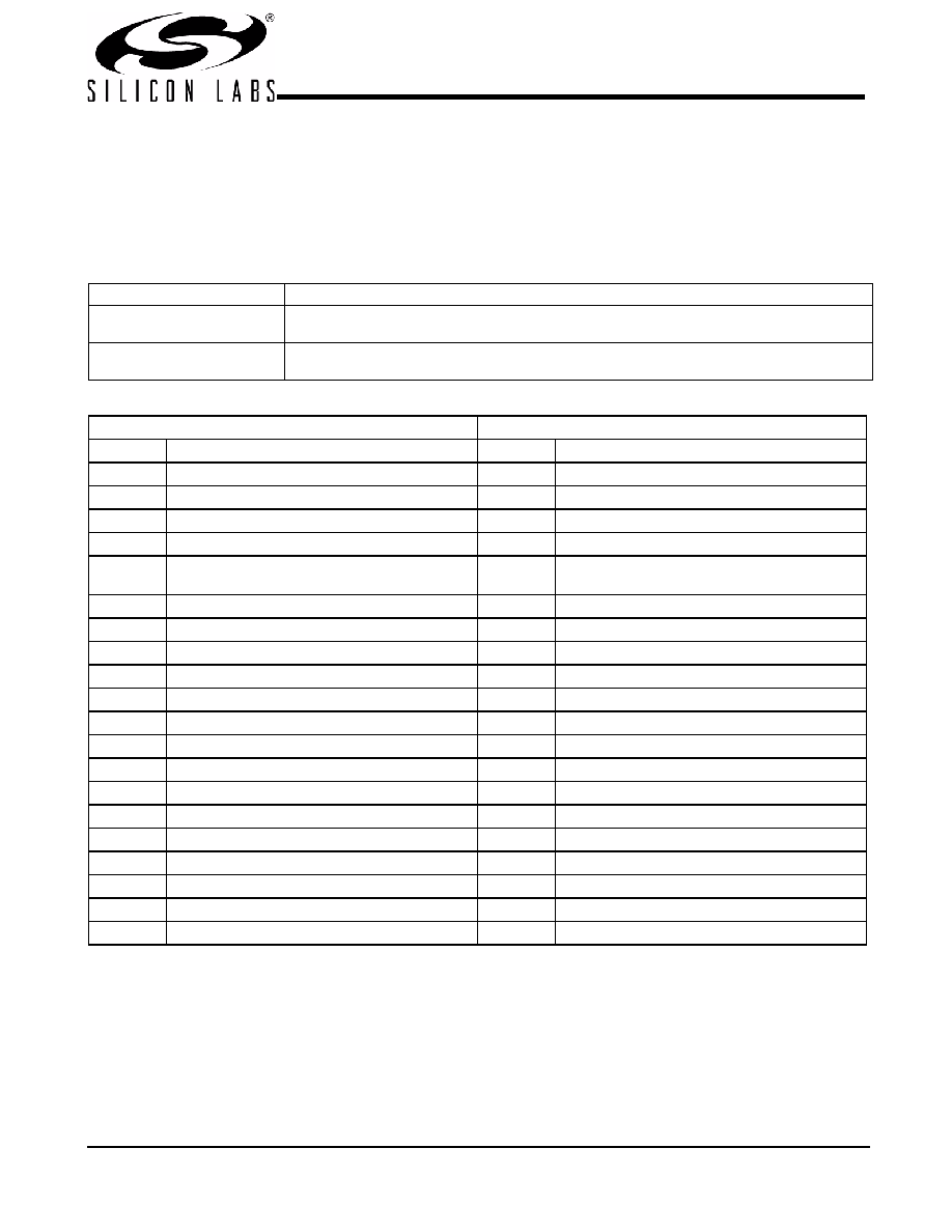
Table 2. Command Code Definition
Bit
Descriptions
7
0 = Block read or block write operation
1 = Byte/Word read or byte/word write operation
6:0
Byte offset for byte/word read or write operation. For block read or write operations, these bits
need to be set at ‘0000000’.
Table 3. Block Read and Block Write Protocol
Block Write Protocol
Block Read Protocol
Bit
Description
Bit
Description
1Start
2:8
Slave address – 7 bits
2:8
Slave address – 7 bits
9Write
10
Acknowledge from slave
10
Acknowledge from slave
11:18
Command Code – 8 bits
‘00000000’ stands for block operation
11:18
Command Code – 8 bits
‘00000000’ stands for block operation
19
Acknowledge from slave
19
Acknowledge from slave
20:27
Byte count – 8 bits
20
Repeat start
28
Acknowledge from slave
21:27
Slave address – 7 bits
29:36
Data byte 0 – 8 bits
28
Read
37
Acknowledge from slave
29
Acknowledge from slave
38:45
Data byte 1 – 8 bits
30:37
Byte count from slave – 8 bits
46
Acknowledge from slave
38
Acknowledge
...
Data byte N/Slave acknowledge...
39:46
Data byte from slave – 8 bits
...
Data byte N – 8 bits
47
Acknowledge
...
Acknowledge from slave
48:55
Data byte from slave – 8 bits
...
Stop
56
Acknowledge
...
Data bytes from slave/Acknowledge
...
Data byte N from slave - 8 bits
...
Not acknowledge
...
Stop
发布紧急采购,3分钟左右您将得到回复。
相关PDF资料
CY28323OXC
IC CLOCK BROOKDALE GPENT4 48SSOP
CY28354OXC-400
IC BUFF 273MHZ 4DDR DIMM 48SSOP
CY28378OXC
IC CLOCK CK408/TITAN 845 48SSOP
CY284108ZXC
IC CLOCK SERV CK410B 56TSSOP
CY28410OXC-2
IC CLOCK CK410 GRANTSDALE 56SSOP
CY28410OXC
IC CLOCK CK410 GRANTSDALE 56SSOP
CY28411ZXC
IC CLOCK CK410M ALVISO 56TSSOP
CY28442ZXC-2
IC CLOCK ALVISO PENTM 56TSSOP
相关代理商/技术参数
CY28317PVXC-2T
功能描述:时钟发生器及支持产品 NB Clk VIA SDRAM Chipsets / Tualatin RoHS:否 制造商:Silicon Labs 类型:Clock Generators 最大输入频率:14.318 MHz 最大输出频率:166 MHz 输出端数量:16 占空比 - 最大:55 % 工作电源电压:3.3 V 工作电源电流:1 mA 最大工作温度:+ 85 C 安装风格:SMD/SMT 封装 / 箱体:QFN-56
CY28317ZC-2
制造商:CYPRESS 制造商全称:Cypress Semiconductor 功能描述:FTG for Mobile VIA PL133T and PLE133T Chipsets
CY28317ZC-2T
制造商:CYPRESS 制造商全称:Cypress Semiconductor 功能描述:FTG for Mobile VIA PL133T and PLE133T Chipsets
CY28322
制造商:未知厂家 制造商全称:未知厂家 功能描述:Clocks and Buffers
CY28322-2
制造商:CYPRESS 制造商全称:Cypress Semiconductor 功能描述:133-MHz Spread Spectrum Clock Synthesizer with Differential CPU Outputs
CY28322ZC-2
制造商:Rochester Electronics LLC 功能描述:- Bulk
CY28322ZC-2T
制造商:Rochester Electronics LLC 功能描述:- Bulk
CY28323
制造商:CYPRESS 制造商全称:Cypress Semiconductor 功能描述:FTG for Intel㈢ Pentium㈢ 4 CPU and Chipsets